What is this about?I see a lot of interest in this forum from folks who experiment with all kinds of RF techniques, antennas and matching etc.
I bragged around that I made a RFM69 clone, which is true but it was just an experiment, which I am sure could be much improved, so this is an effort to reach out to the RF experts and ask them to voice their RF wisdom and share advice. I don't have the expensive RF tools to do tests or measure loads matching etc (VNAs and whatnot).
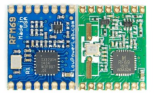
Here's my version of the RFM69 next to Hope's:
 Some more background
We've seen
threads like this one where discussion starts to go into the details of the RFM69/semtech design of the module.
HopeRF has a sx1231h board that has followed the Semtech design almost to the letter but they cut a few corners to allow the same PCB to assemble into a RFM69W or RFM69HW. They add a few components like a transistor to invert the RF switch control.
They use a specific GaAs RF switch (the G4C marked SC70 package chip) which is discontinued but they seem to have vast amounts of this or source it from asia somehow since all the radios I see many of their radios contain this RF switch (for instance the LoRa radios, HW radios, RFM22b etc). The W radios (13dbm like RFM69W) do not contain this switch or the transistor that drives it and the reason is obvious from the transceiver DS, and has a slightly different output path but uses the same PCB.
One thing that confuses lots of people is the main chip used on the RFM69 which is marked as
"RF69". This is a custom QFN28 packaged sx1231h, instead of the original QFN24
"SX1231h" which you can buy from digikey, see photo above for comparison and package pin count difference.
This blue board I made can be used to make Ws or HWs. I used a RF switch that had the logic table inverted so I didn't need the extra transistor+resistor driving it.
SX1231h DatasheetRF Switch on the RFM69 DatasheetWhat I'd like to focus in this discussion:- use the sx1231h chip to design a board that is 100mW capable, similar to the blue one above
- discuss whether it's worth using a common PCB that can morph into a W or HW or whether optimizing the design for a single variant can reduce any losses and make a better module
- discuss the possibility of a 4 layer and what the real gains are - middle layers would have GND and VCC to follow RF design patterns and minimize capacitive coupling etc
- discuss the necessity of a metal can cover
- discuss the possibility of replacing the matching network with a single component - i've seen these on some RF boards but I don't know what/how/if this can replace the many 0402 components. If it's possible this would reduce complexity, perhaps reduce losses, maybe even cost
- RF chips usually are very dense and use 0402 components as industry standard, but we've seen the RFM12b using 0603 which is MUCH less challenging to assemble on a pick and place
- pinout should be unchanged, with the exception that the NC (not connected pin) could be used for something useful like telling the difference between a W and HW, which could then be used in software (a logical HIGH on that pin could mean HW for instance)
- substrate PCB should be no thicker than 1mm
- of course, made in the USA

- price will be more for many reasons: a basic BOM is easily a few dollars (sx1231h, good quality crystal, rf switch). The quest here is to see if a better design is possible and if the tradeoff with cost makes it justifiable to produce.
I will add to this list as ideas come up.
Please share your advice, RF experts!Let's watch this space produce something great, but keeping it focused, with information backed by experience and data.


